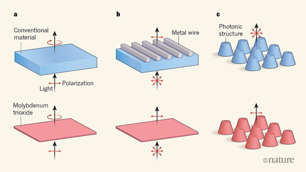
The optical properties of materials
In my group we study the properties of a wide range of materials, including wide band gap semiconductors, charge denisty wave materials and 2D materials. In particular, we are interested in creating new types of polariton modes, which have behaviour seen not in conventional materials. We are also interested in using infrared spectroscopic techniques to understand materials which support condensed matter states, such as charge denisty waves.
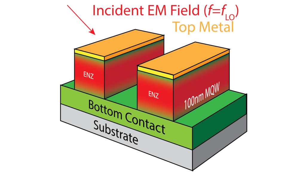
Enhanced infrared optoelectronics
The concepts of nanophotonics can be directly appplied to the creation of infrared light sources and detectors. Current infrared technology only operates at well below room temperature, however nanophotonics allows us to make devices smaller and more efficient. Infrared detectors form the basis of thermal imaging, and can be applied in areas from defence to enviromental monitoring.
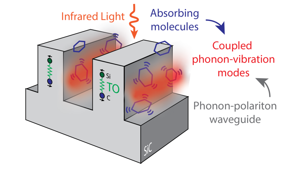
Vibrational sensing and strong coupling
One of the applications for nanophotonics is in the detection of small ammounts of biological toxins and molecules. In my group we use polaritons to enhance the coupling of light to the vibrations of different molecules. If pushed far enough, the cavity enters what is known as the strong coupling regieme, which can give rise to new behaviour from the molecules.
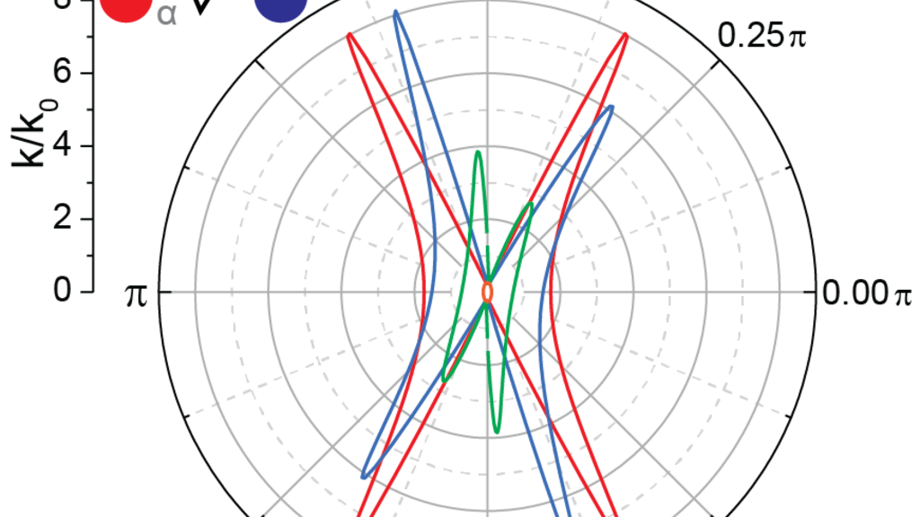
NSF Career - CAREER: Photonics in the Lowest Symmetry Crystals
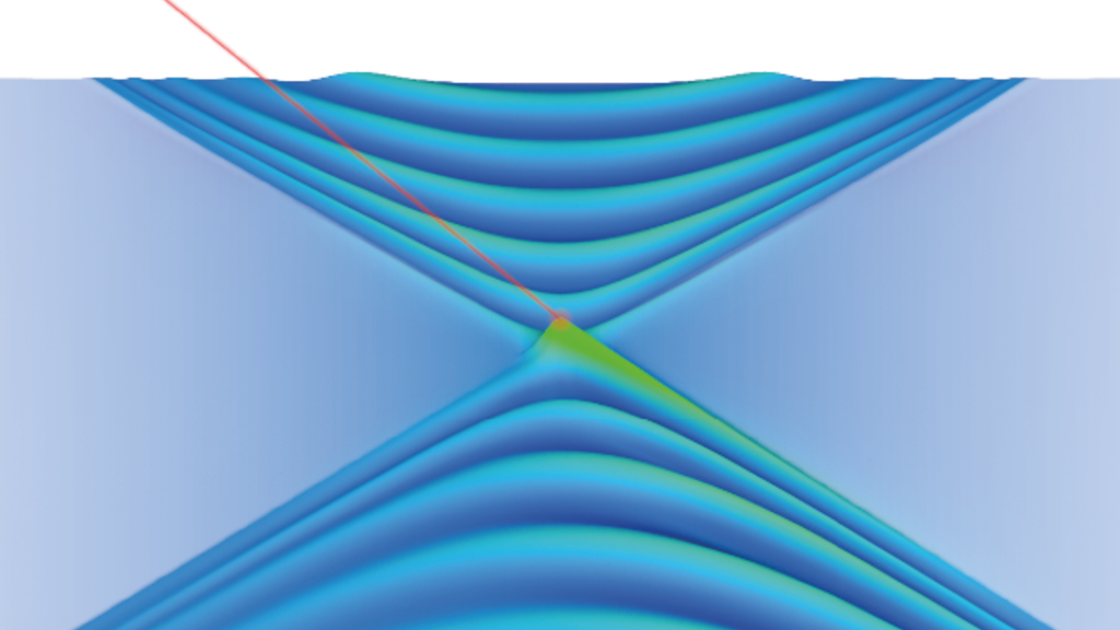
Research on Hyperbolic Shear Polaritons published in Nature
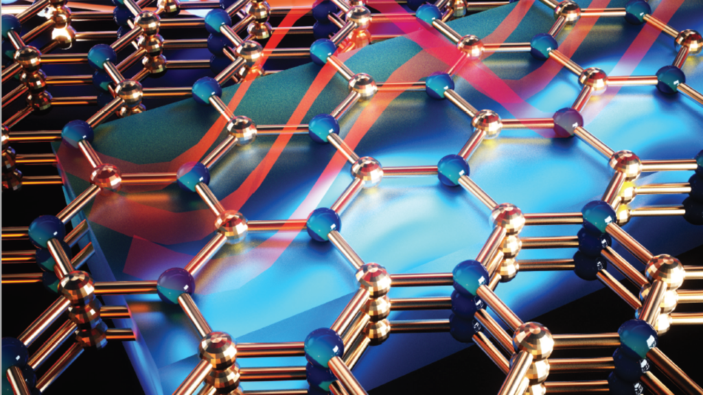
Hybrid Mid-Near Infrared Waveguides

Perspective on new concepts for infrared optoelectronics

Superstructure Emitters published in APL
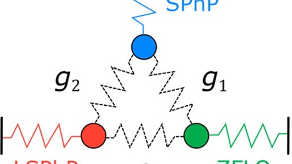
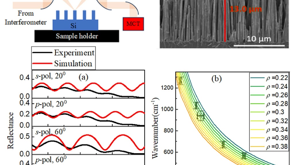
Work on non-destructive spectroscopy of Si nanowires published
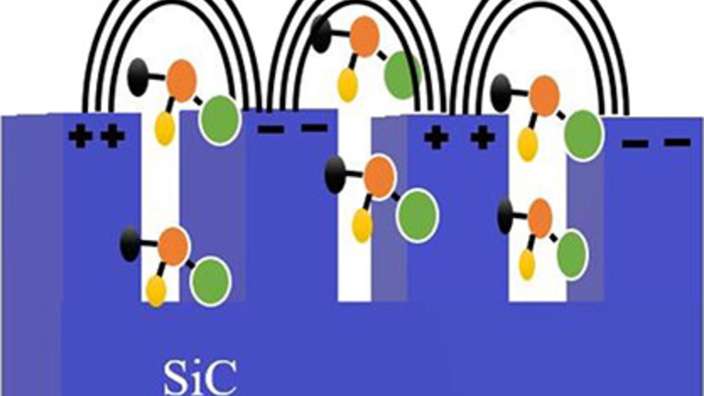
New paper 'Lifetime and Molecular Coupling in Surface Phonon Polariton Resonators'
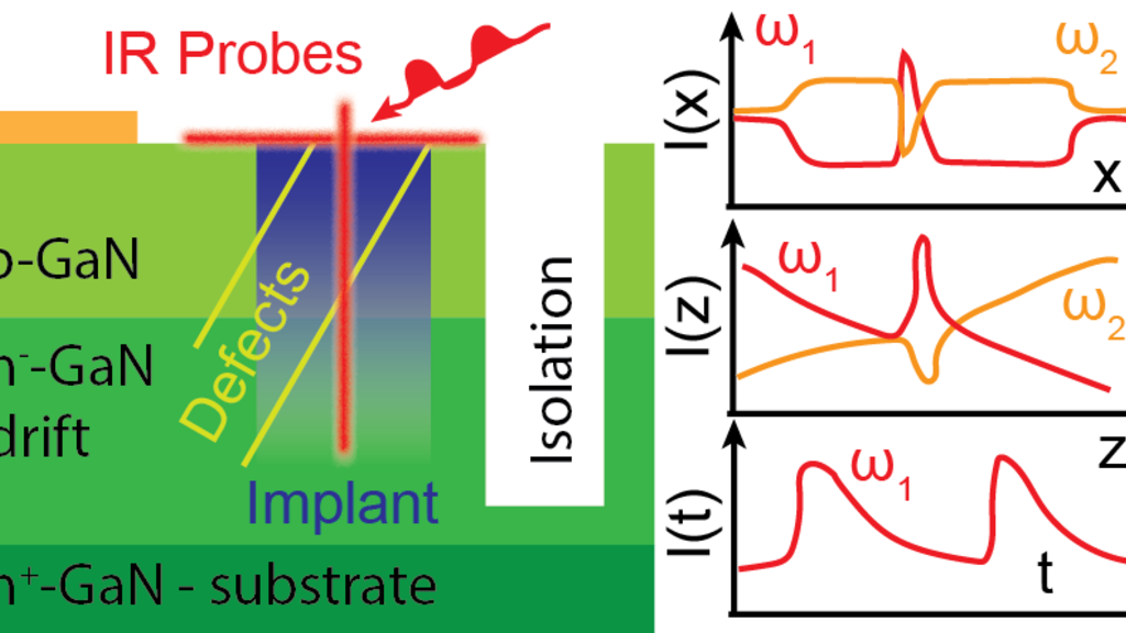
New ONR award to studying GaN using infrared spectroscopy
Nanofabrication
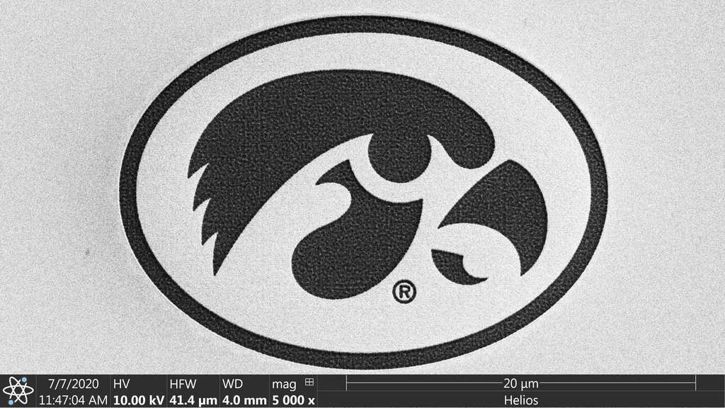
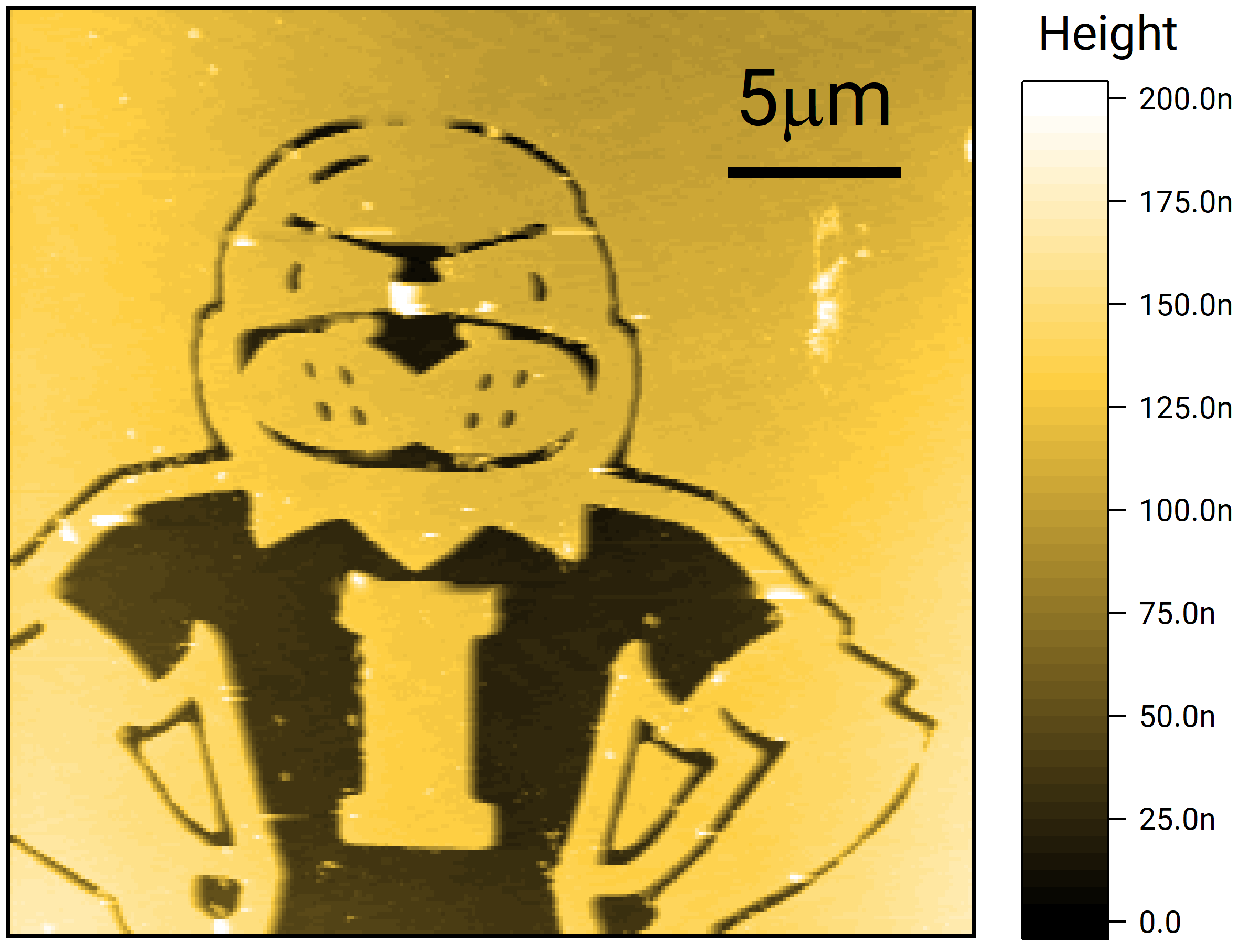
In my group we use micro- and nanofabriaction proecess in order to fabricate optical structures and devices. We use a combination of lithography, depsotion and transfer techniques in order to realize complex structures at the nanoscale. Above we show a micron scale Iowa logo, made used focussed ion beam lithography. Below we show Herky made using photolithography and imaged using our AFM
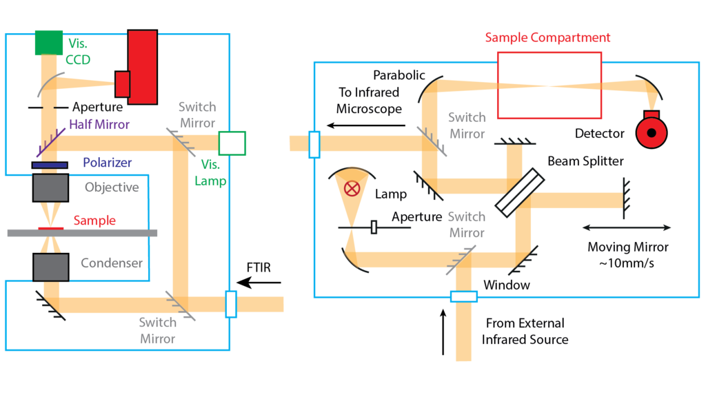
Infrared Spectroscopy
In order to determine the properties of the materials we study we use infrared spectroscopy. This uses a Michelson Interferometer to measure the optical properties of materials from the near infrared through to the far infrared, encompassing the energies of crystal vibrations, intraband transitions in semiconductors, and semiconductor band gaps.