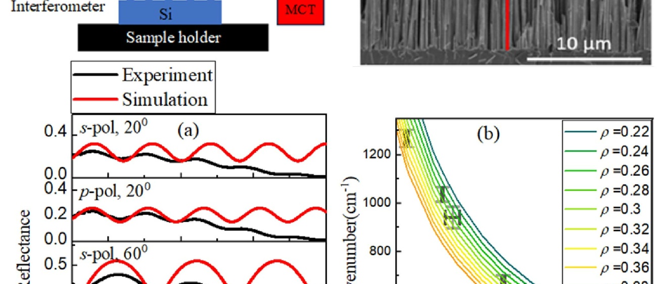
Silicon nanowires (SiNWs) have attracted much attention owing to their potential applications in electronics and photonics, while remaining as a cost-effective material platform. Key material properties in engineering SiNWs for different applications include their length, density, and presence of oxides or other chemicals on the surface. However, monitoring these properties is challenging, as scanning electron microscopy and atomic force microscopy (AFM), which directly image the wires, require destructive cleaving of the sample. This paper uses polarized, variable-angle Fourier Transform IR reflectance spectroscopy as a nondestructive technique to characterize the areal density and length of metal-assisted chemically etched SiNW arrays. In addition to the ability to characterize “as-etched” wires, we show that IR spectroscopy can also measure few-nanometer thick layers of aluminum oxide (AlOx) grown radially around the length of the SiNWs utilizing atomic layer deposition. Despite sample inhomogeneities, an effective medium theory (EMT) model can determine the length and density of the NWs for a range of lengths between 3 and 14 μm. The EMT can also reproduce the experimentally measured vibrational bands for coated NWs, demonstrating that IR spectroscopy can also evaluate the presence of molecular contaminants on the wires.
Work combines efforts from the Folland and Toor groups.
Wednesday, November 20, 2024
